|
Introduction
Damage was first identified in a couple of surface mounted
diodes, see Figure 2.10-2 below, which are near the switch
mode power supply connector.
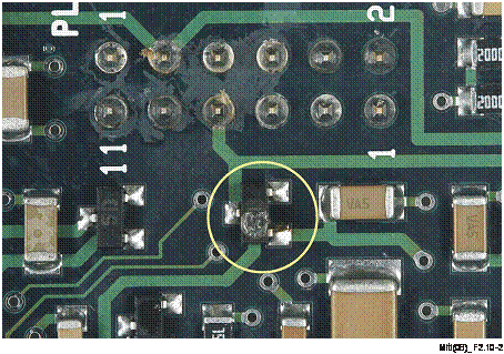
Figure 2.10-2 – Picture of damaged diode
Circuits, schematics and printed circuit board (PCB)
layouts were obtained for this part of the system. This
information, in combination with installation documentation,
enabled a scenario for damage to be determined. It also
identified components likely to be damaged. These components
were:
- a thyristor protection circuit, which is a switching
type protector and the first component on the printed circuit
board where the line terminates;
- a diode which clamps the incoming line to the –70 V
supply rail (line);
- a diode which clamps the incoming line to the –35 V rail
(line);
- two diodes which connect from the –35 V and –70 V supply
lines to the SLIC circuit. One of these diodes is shown
damaged in Figure 2.10-2 above;
- the SLIC circuit.
Investigation
The scenario is that a negative surge exceeding –70 V will
drive the –70 V supply more negative due to current being
conducted via the diode which clamps the incoming line to the
–70 V supply rail. If the –70 V rail becomes too negative, it
can cause semiconductor "latch up" of the SLIC. "Latch up" is
a failure mechanism in semiconductor devices where externally
applied transients exceeding the maximum supply voltage
result in the triggering of internal parasitic transistors
forming a thyristor-type structure. This internal thyristor
can conduct appreciable current and typically results in the
rapid destruction of the device.
The network operator investigated damage to the external
thyristor protection circuit, to the diode which clamps the
incoming line to the –70 V supply rail, and to the SLIC, by
electrically characterizing these components and then
de-encapsulating those components with degraded
characteristics and inspecting them under an optical
microscope. The SLIC showed signs of significant damage
consistent with "latch up" indicating that the power supply
was supplying current conducted to ground via the SLIC. The
thyristor protection circuit had no signs of damage.
Surges were applied to a working circuit to verify this
scenario. Figure 2.10-3 shows negative surges applied to an
unprotected circuit. The generator surge (–191 V) causes a
surge of –100 V on the b leg of the circuit. The difference
of 91 V is due to the voltage drop on the coupling metal
oxide varistor (MOV). The surge has caused the –70 V rail to
be driven more negative (–70 V to
–96 V). After a few surges, permanent damage has occurred.
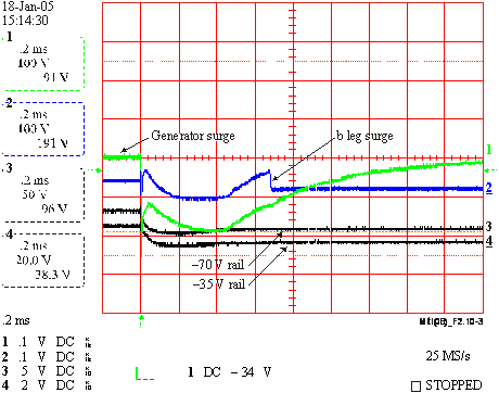
Figure 2.10-3 – Waveforms during a damaging surge
The failure appears to be caused by a negative surge
entering under the firing voltage of the thyristor protection
circuit (±190 V) and causing the –70 V and the –35 V rails to
become more negative by the current entering the power supply
via the diode which clamps the incoming line to the –70 V
supply rail. When the –70 V rail is surged to approximately
–100 V and the –35 V rail is surged to approximately –45 V,
the SLIC latches up and the current is conducted from the –70
V and –35 V rails to ground, see Figure 2.10-4, which shows
the current path through the thyristor protection circuit and
the diode to –70 V, and the current from the –70 V and –35 V
rails through the SLIC. It is the power supply current that
damages the two diodes which connect from the –35 V and –70 V
supply lines to the SLIC circuit (based on the fact that the
diode which clamps the incoming line to the –70 V supply rail
is not damaged).
The diode which clamps the incoming line to the –70 V
supply rail was probably added to prevent the SLIC line
inputs exceeding –70 V. However, adding this diode has
resulted in rendering the thyristor protection circuit
redundant and causing the SLIC to have its –70 V and –35 V
ratings exceeded.
The scenario was confirmed by applying surges to a working
circuit.
Investigation
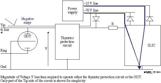
Figure 2.10-4 – Simple circuit showing path of surge on
tip side of line
|