|
Identifying failed components
The first part of the investigation was to identify the
damaged components using normal service techniques. The
component most damaged was a transmission IC. The plastic
coating on top of the IC was then removed using chemical
etching to expose the die. The die was then inspected using
an optical microscope and photographed. Typical field damage
can be seen in Figure 2.7-2.
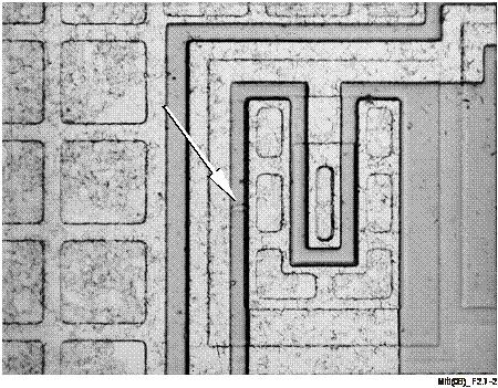
Figure 2.7-2 – Damage to the transmission IC by lightning
strikes
This damage is due to a breakdown between a conductor
track and a ground as a result of an impulse overvoltage.
Replicating field damage in the laboratory
In an attempt to replicate this damage, different types of
lightning surges, as recommended in Rec. ITU-T K.21, were
applied to the telephone. No damage could be caused using up
to 4 kV 10/700 µs waveshape, without external surge
protective devices (SPDs), i.e., an inherent test voltage of
4 kV. When the voltage was further increased, damage could be
caused but it was a different type of damage.
The next type of test was to investigate whether the
operation of a GDT or sparkgap could cause a very high dV/dt
and replicate damage to the IC. This test was performed with
a GDT or sparkgap across the line or line to earth. Voltages
as high as 6 kV could not damage the IC.
The next experiment was to check if high voltages (up to
100 kV) applied longitudinally could cause high charging
currents and damage the IC due to the capacitance of the
phone to earth. The charging currents did not cause damage
but when one side of the line discharged to earth, the damage
was replicated. The current waveform of the current
conducted transversely through the phone, when one side of
the line breaks down, is as shown in Figure 2.7-3. This
waveshape caused similar damage to the audio IC compared with
field damaged ICs.
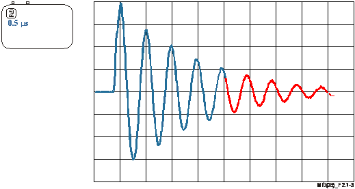
Figure 2.7-3 – Current waveshape
entering the phone to replicate field damage
Increasing the resistibility of the phone
To "harden" the phone against damage, the current path
from the line into the IC was identified from knowing the
entry pins on the IC. The circuit was redesigned to minimize
inductance of SPD lead lengths and components added to
minimize the amount of current which could enter the IC. The
inherent resistibility of the phone was increased fourfold
from approximately 200 A to 800 A. Hardening the phone to
this level eliminated damage to the phone, saving millions of
dollars in maintenance per annum.
Unfortunately, while damage was no longer occurring,
customers began complaining about stored number loss. Stored
number loss was replicated by using the waveshape above but
with a very high frequency oscillation added to the first
half cycle.
The test generator used for the hardware damage test and
the memory loss test is given in Figure 2.7‑4.
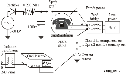
Figure 2.7-4 – Test generator for
hardware damage and memory loss test
Lead lengths
The lead resistances and inductances are critical factors
in determining the maximum current amplitude obtainable for a
given generator source voltage and hence, the shorter the
lengths (phone & earth) involved, the less source voltage
required.
Test method
- Hardware component test: Spark gap 2 shall be
closed. Spark gap 1 shall be opened to 1 mm. The voltage
source for the generator shall be slowly increased until
breakdown just occurs across Spark gap 1. The breakdown
across the spark gap will be repeated as the capacitor
recharges and discharges. The peak-to-peak current, of the
first cycle, flowing to ground shall be measured and noted.
The waveform shall be the same as the ringwave. The phone
shall be subjected to 10 ringwave impulses before the
telephone is tested for correct operation. Spark gap 1
shall then be opened in 1-mm steps and the process repeated
until a peak current of 800 A is achieved. This is the
current that the telephone is expected to resist without
damage or misoperation. A new phone sample may be tested at
this point to remove any deleterious combined effects of
previous testing.
- Memory retention test: The opening of Spark gap
1 shall be adjusted to achieve a peak current of 400 A. It
will be necessary to reduce the source voltage until a
controlled discharge repetition rate is achieved. Once this
current has been achieved, Spark gap 2 shall be opened to 2
mm. A minimum of 10 ring-wave impulses shall be performed
on the telephone after which correct operation and memory
retention shall be confirmed.
NOTE – The first half cycle of this ringwave will have a
very high frequency ring wave superimposed on it. No attempt
should be made to characterize this very high frequency ring
wave as it would be exceeding the oscilloscope and current
transformers operational performance parameters. Furthermore,
it would require specialist measurement techniques, which are
beyond the scope of this handbook.
Surge coupling
Because half of the services had GDTs installed, it is
assumed that the coupling must have taken place between the
phone and the GDT. Two methods have been thought of:
- Induction into the internal cabling: This is thought
unlikely as the surge is a transverse current requiring
breakdown to ground of one side of the cable. This would
require an induced voltage of tens of kilovolts.
- Breakdown from earth to one side of the cable due to a
high earth potential rise (EPR) due to a close ground
strike: In Australia, indoor cabling is often tacked under
the floor of the building and hence breakdown is possible.
|