
Page 24 - ITU Journal, Future and evolving technologies - Volume 1 (2020), Issue 1, Inaugural issue
P. 24
ITU Journal on Future and Evolving Technologies, Volume 1 (2020), Issue 1
tenna between different values (or states). This in turn
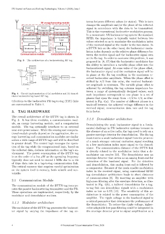
RF energy harves�ng module
changes the amplitude and/or the phase of the reflected
Power Power signal in accordance with the data to be transmitted.
Harves ng Management Supercapacitor This is the conventional backscatter modulation process.
Vdd
In a monostatic AR backscattering system like standard
Demodulator Computa onal RFID, the impedance is typically varied between two
Logic
Comm values selected so as to maximize the modulation index
Control of the received signal at the reader in the two states. In
Modulator Memory a BTTN link on the other hand, the backscatter modu-
lation index depends on the relative phase difference be-
Communica�on module Computa�on module tween the exciter signal and the backscatter signal seen
at the Rx tag. In order to overcome this problem, it was
Fig. 3 – The architecture of a backscattering RF tag. proposed in [8, 17] that the backscatter modulator has
the ability to introduce a variable phase offset into the
Comm &
Data Ctrl backscattered signal. At some value of the phase offset,
Antenna Antenna
Ctrl ZL1 the backscatter signal and the excitation signal will be
ZL2 in phase at the Rx tag resulting in the maximum re-
Envelope Amplifier + Comparator rxData ceived backscatter amplitude. When the phase offset is
Detector BP filter
ZLn shifted by /2 from this value, the received backscat-
(b)
ter amplitude is minimum. The variable phase offset is
RF Switch
achieved by switching the tag antenna impedance be-
(a)
tween a range of systematically designed values; each
Fig. 4 – Circuit implementation of (a) modulator and (b) demod-
ulator backscattering-based RF tag. such impedance corresponds to one phase in a set of
phases that span the range from − /2 to /2, as illus-
tributions to the backscatter PR tag-to-tag (T2T) links trated in Fig. 4(a). The number of different phases is a
are summarized in Table 1. trade-off between the achieved voltage difference in the
received signal, communication data rate and the tag
3. TAG HARDWARE form factor.
The overall architecture of the BTTN tag is shown in
Fig. 3. It has three modules, a communication mod- 3.1.2 Demodulator architecture
ule, an energy harvesting module, and a computation Demodulating the weak backscatter signal is a funda-
module. The tag optionally interfaces to an external mental challenge in PR backscatter systems because in
near-zero power sensor. While the sensing and computa- the absence of an active radio, the tags need to rely on a
tional module greatly depend on the application, the en- passive envelope detector for demodulation. The Rx tag
ergy harvesting and communication modules are similar must resolve a weak backscatter signal from the presence
across a wide range of BTTN tags and will be described of a much stronger external excitation signal resulting
in greater detail. The control logic manages the opera- in a low modulation index input signal to the demod-
tion of the tag while the computational logic, based on ulator. The communication distance of the BTTN link
the collected data, deduces information on the tag’s en- is directly related to the modulation index that a de-
vironment. The power consumption of the BTTN tag modulator can resolve [13]. The demodulator uses an
is on the order of a few W as the operating frequency envelope detector that serves as an analog front-end for
typically does not need to exceed 1 MHz due to a 10s extraction of the baseband signal. For the detection
of kbps data rate in a tag-to-tag communication link. and demodulation, this analog front-end is followed by
The critical resource that requires careful optimization a comparator. Because of the much smaller modulation
on the system level is memory, both volatile and non- index in the received signal, using conventional RFID
volatile. tag demodulator architecture leads to short distances
of communication [9]. By inserting an amplifier with
3.1 Communication Module high-pass filtering after the envelope detection, as illus-
The communication module of the BTTN tag incorpo- trated in Fig. 4(b), a tailored demodulator for a tag-
rates the passive backscattering transmitter and the PR. to-tag link can demodulate signals with a modulation
These operations are implemented, respectively, by the index as low as 0.5% [13]. The sensitivity of this ar-
modulator and demodulator sections. chitecture is related to the power consumption of the
amplifier. The ripple voltage in the baseband signal is
3.1.1 Modulator architecture a critical parameter that determines the performance of
the demodulator. To reduce the ripple voltage, higher-
The modulator of the BTTN tag generates the backscat- order adaptable low-pass filtering could be integrated in
ter signal by varying the impedance of the tag an- the envelope detector prior to signal amplification at a
4 © International Telecommunication Union, 2020